The achievement of the proposed objectives can only be fulfilled through a well-coordinated effort within the consortium and a coherent work breakdown structure, in accordance to the targeted level of maturity of the demonstrators. The project is completely organized in a top-down approach: all the activities are driven by the needs of the end-users, reflected in the specifications of the demonstrators. The strategy allows each end-users to express its specific needs in order to maximise the industrial impact of the project.The work breakdown structure of the project and the dependencies of the inter-related WPs are depicted in the following figure
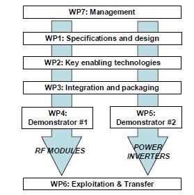
In WP 1 Specifications and Design, product specifications and associated technologies specifications will be produced to start the project. Then, all the technology and packaging developments will be reported into system level simulations to continuously monitor the project progress toward the industrial project goals. WP 2 is dedicated to the development of key enabling technologies. These key technologies are transverse and will the serve all the applications. They will enable the integration of the SiC and GaN chips into their specific packages with the required high power handling thanks to a leverage effect on specific packaging-related issues:- ThermoElectric modules to address transient and hot-spot cooling in harsh environments- Thermal Interface Materials with low thermal resistance and high reliability, crucial in the attaching process of the chips and in their thermal connection to the packages- Electrical Interconnect to establish electrical contact through the packages- Heat spreading materials to relax heat density- T° sensors that are monolithically integrated as close as possible to the junction to monitor and control the operating temperature. WP 3 is dedicated to integration and packaging aspects. Partners will lead the development of new packaging solutions specifically adapted to the end-user needs. On one hand, the set of power inverters demonstrators need a packaging solution compliant with SiC technology and will integrate micro-Pelletier modules. On the other hand, a compact and reliable packaging solution will be developed for RF applications while being compliant with GaN power amplifier technology and the integration of a T° sensor. These tasks will be supported by stress measurement techniques
WP 4 is dedicated to the fabrication of the RF module demonstrator (a 25W emitter using GaN High PowerAmplifier) for aerospace applications. Performance and reliability evaluations will be carried out. In WP 5, three demonstrators of industrial power inverters are undertaken under the lead of Schneider-Electric through a close collaboration with a historically natural and favoured partner Infineon. This work-package is organized in three tasks corresponding to the development of three incremental demonstrators in order to reduce the technological risk. The project also includes a work package WP 6 devoted to dissemination and exploitation activities. The aim is not only to ensure the dissemination of the project results toward the relevant industrial communities but overall to guarantee the industrial transfer of the developed technologies and to secure the corresponding supply chain. Finally, management activities are grouped into WP 7 and drive all types of activities: technical, administrative,organizational, etc.

The SMARTPOWER project is co-funded by the European Commission under the "Information and Communication Technologies" Seven Framework Programme under the Grant Agreement No 288801
 A propos de SmartPower
Developing new packaging for the thermal management of SiC- and GaN-based power modules in an efficient and cost-effective way